DWM1001C
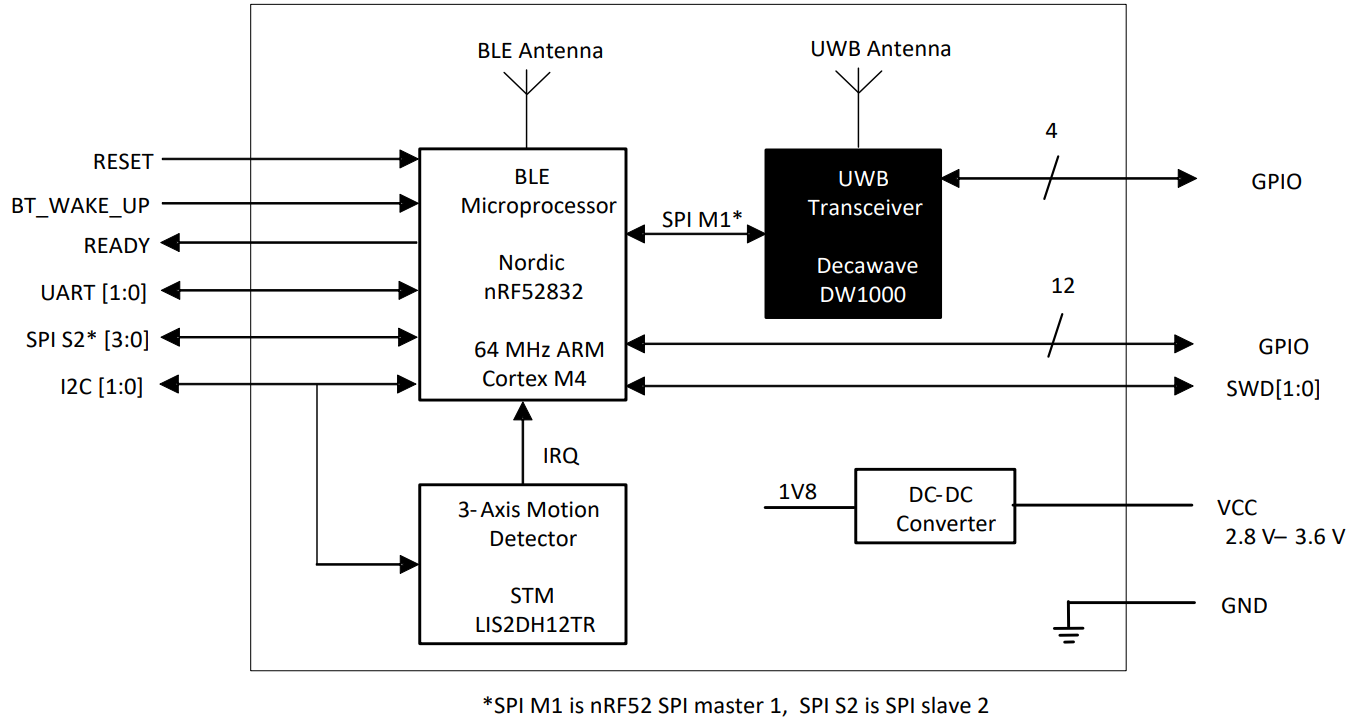
The DWM1001 module is based on Decawave’s DW1000 Ultra Wideband (UWB) transceiver IC, which is an IEEE 802.15.4-2011 UWB implementation. It integrates UWB and Bluetooth® antenna, all RF circuitry, Nordic Semiconductor nRF52832 and a motion sensor.
Note
To get more information, please visit the Qorvo’s DWM1001C page.
Key Features
Ranging accuracy to within 10cm.
The UWB Channel 5 printed PCB antenna (6.5 GHz)
6.8 Mbps data rate IEEE 802.15.4-2011 UWB compliant
Nordic Semiconductor nRF52832
Bluetooth® connectivity
Bluetooth® chip antenna
Motion sensor: 3-axis accelerometer
Current consumption optimized for low power sleep mode: <15μA
Supply voltage: 2.8 V to 3.6 V
Size: 19.1 mm x 26.2 mm x 2.6 mm
Modules marked DWM1001C are certified to ETSI, FCC and ISED regulations
FCC ID: 2AQ33-DWM1001, IC: 23794-DWM1001.
See the module marking section of this datasheet.
Software Compatibility
It is compatible with both LEAPS RTLS and PANS PRO RTLS.
Block Diagram
Pinouts Description
Pin Numbering
DWM1001 module pin assignments are as follows (viewed from top): -
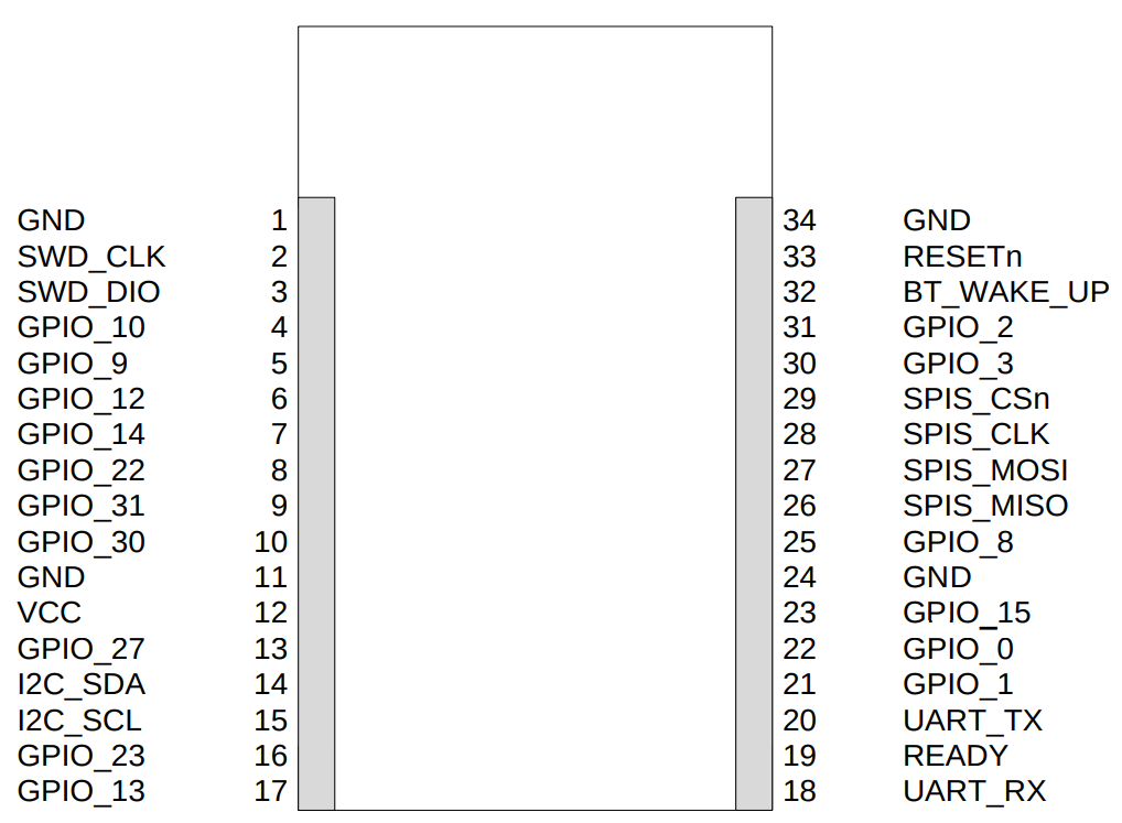
Pin Descriptions
Pin details are given in
SIGNAL NAME
PIN
DESCRIPTION
SWD_CLK
2
DI
Serial wire debug clock input for debug and programming of Nordic Processor
[N] SWDCLK
SWD_DIO
3
DIO
Serial wire debug I/O for debug and programming of Nordic Processor
[N] SWDIO
GPIO_10
4
DIO
General purpose I/O pin.
[N] P0.10
GPIO_9
5
DIO
General purpose I/O pin.
[N] P0.9
GPIO_12
6
DIO
General purpose I/O pin.
[N] P0.12
GPIO_14
7
DIO
General purpose I/O pin.
[N] P0.14
GPIO_22
8
DIO
General purpose I/O pin.
[N] P0.22
GPIO_31
9
DIO
General purpose I/O pin. ADC function of nRF52
[N] P0.31
GPIO_30
10
DIO
General purpose I/O pin. ADC function of nRF52
[N] P0.30
GPIO_27
13
DIO
General purpose I/O pin.
[N] P0.27
I2C_SDA (Master)
14
DIO
Master I2C Data Line.
[N] P0.29
I2C_SCL (Master)
15
DO
Master I2C Clock Line.
[N] P0.28
GPIO_23
16
DIO
General purpose I/O pin.
[N] P0.23
GPIO_13
17
DIO
General purpose I/O pin.
[N] P0.13
UART_RX
18
DI
UART_RX
[N] P0.11
READY
19
DO
Generated interrupt from the device. Indicates events such as SPI data ready, or location data ready. See the function dwm_int_cfg() in the DWM1001 Firmware API Guide for details[5].
[N] P0.26
UART_TX
20
DO
UART_TX, This is also the ADC function of the nRF52
[N] P0.05
GPIO_1
21
DIO
General purpose I/O pin of the DW1000. It may be configured for use as a SFDLED driving pin that can be used to light a LED when SFD (Start Frame Delimiter) is found by the receiver. Refer to the DW1000 User Manual [1] for details of LED use.
[DW] GPIO1
GPIO_0
22
DIO
General purpose I/O pin of the DW1000. It may be configured for use as a RXOKLED driving pin that can be used to light a LED on reception of a good frame. Refer to the DW1000 User Manual [1] for details of LED use
[DW] GPIO0
GPIO_15
23
DIO
General purpose I/O pin.
[N] P0.15
GPIO_8
25
DIO
General purpose I/O pin.
[N] P0.08
SPIS_MISO
26
DI
Configured as a SPI slave this pin is the SPI data output. Refer to Datasheet for more details [1].
[N] P0.07
SPIS_MOSI
27
DO
Configured as a SPI slave this pin is the SPI data input. Refer to Datasheet for more details [1].
[N] P0.06
SPIS_CLK
28
DI
Configured as a SPI slave this pin is the SPI clock. This is also the ADC function of the nRF52
[N] P0.04
SPIS_CSn
29
DI
Configured as a SPI slave this pin is the SPI chip select. This is an active low enable input. The high-to-low transition on SPICSn signals the start of a new SPI transaction. This is also the ADC function of the nRF52
[N] P0.03
GPIO_3
30
DO
This pin is configured for use as a TXLED driving pin that can be used to light a LED during transmit mode. Refer to the DW1000 User Manual [2] for details of LED use.
[DW] GPIO3
GPIO_2
31
DO
This pin is configured for use as a RXLED driving pin that can be used to light a LED during receive mode. Refer to the DW1000 User Manual [2] for details of LED use.
[DW] GPIO2
BT_WAKE_UP
32
DI
When this pin is asserted to its active low state the Bluetooth device will advertise its availability for 20 seconds by broadcasting advertising packets. This is also the ADC function of the nRF52.
[N] P0.02
RESETn
33
DI
Reset pin. Active Low Input.
[N] P0.21
VCC
12
P
External supply for the module. 2.8V - 3.6V
.
GND
1, 11, 24, 34
G
Common ground.
.
Explanation of Abbreviations
ABBREVIATION
EXPLANATION
DI
Digital Input
DIO
Digital Input / Output
DO
Digital Output
G
Ground
P
Power Supply
N
nRF52832
DW
DW1000
Note
Any signal with the suffix ‘n’ indicates an active low signal.