LM8
This page offers the basic information about LM8 module
Key Features
Software Compatibility
It is compatible with both LEAPS RTLS and PANS PRO RTLS.
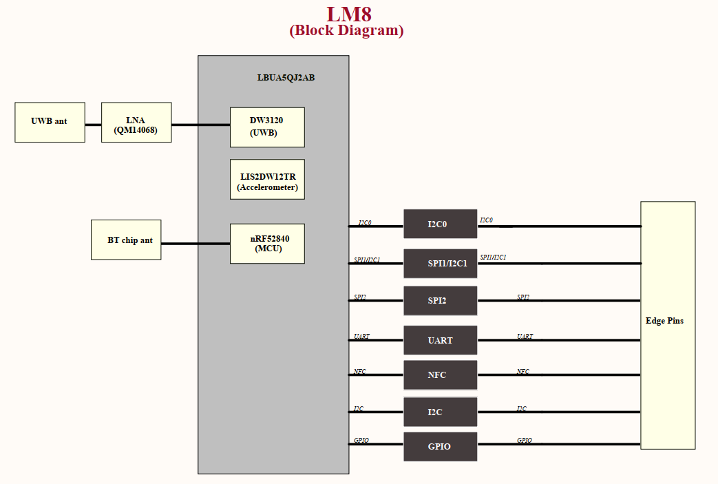
Block Diagram
Pinouts Description
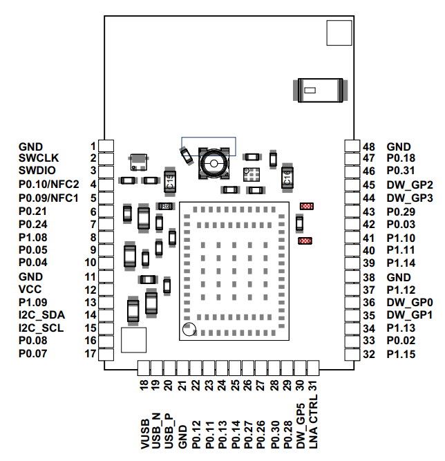
Pin Numbering
LM8 module pin assignments are as follows (viewed from top):
Pin Descriptions
Signal Name |
Pin |
I/O (Default) |
Description |
IC Pin Reference |
|---|---|---|---|---|
Digital Interface |
||||
SWD_CLK |
2 |
DI |
Serial wire debug clock input for debug and programming of Nordic Processor. |
SWD_CLK |
SWD_DIO |
3 |
DIO |
Serial wire debug I/O for debug and programming of Nordic Processor. |
SWD_DIO |
GPIO_1/NFC1 |
4 |
Mixed |
General purpose I/O pin for nRF52840 processor. NFC antenna connection. |
P0.10 |
GPIO_2/NFC2 |
5 |
Mixed |
General purpose I/O pin for nRF52840 processor. NFC antenna connection. |
P0.09 |
GPIO_3 |
6 |
DIO |
General purpose I/O pin for nRF52840 processor. |
P0.21 |
GPIO_4 |
7 |
DIO |
General purpose I/O pin for nRF52840 processor. |
P0.24 |
GPIO_5 |
8 |
DIO |
General purpose I/O pin for nRF52840 processor. |
P1.08 |
GPIO_6 |
9 |
DIO |
General purpose I/O pin for nRF52840 processor. |
P0.05 (AIN) |
GPIO_7 |
10 |
DIO |
General purpose I/O pin for nRF52840 processor. |
P0.04 (AIN) |
GPIO_8 |
13 |
DIO |
General purpose I/O pin for nRF52840 processor. |
P1.09 |
I2C_SDA |
14 |
DIO |
I2C Data Line |
I2C_SDA |
I2C_SCL |
15 |
DO |
I2C Clock Line |
I2C_SCL |
GPIO_9 |
16 |
DIO |
General purpose I/O pin for nRF52840 processor. |
P0.08 |
GPIO_10 |
17 |
DIO |
General purpose I/O pin for nRF52840 processor. |
P0.07 |
VUSB |
18 |
P |
Power Supply(4.4~5.5V) for MCU USB 3.3V Regulator |
VUSB |
USB_N |
19 |
DIO |
USB D- I/O for nRF52840 processor. |
USB_N |
USB_P |
20 |
DIO |
USB D+ I/O for nRF52840 processor. |
USB_P |
GPIO_11 |
22 |
DIO |
General purpose I/O pin for nRF52840 processor. |
P0.12 |
GPIO_12 |
23 |
DIO |
General purpose I/O pin for nRF52840 processor. |
P0.11 |
GPIO_13 |
24 |
DIO |
General purpose I/O pin for nRF52840 processor. |
P0.13 |
GPIO_14 |
25 |
DIO |
General purpose I/O pin for nRF52840 processor. |
P0.14 |
GPIO_15 |
26 |
DIO |
General purpose I/O pin for nRF52840 processor. |
P0.27 |
GPIO_16 |
27 |
DIO |
General purpose I/O pin for nRF52840 processor. |
P0.26 |
GPIO_17 |
28 |
DIO |
General purpose I/O pin for nRF52840 processor. |
P0.30 |
GPIO_18 |
29 |
DIO |
General purpose I/O pin for nRF52840 processor. |
P0.28 |
DW_GP5 |
30 |
DW |
General purpose I/O of QM33120W |
DW_GP5 |
LNA CTRL |
31 |
DW |
General purpose I/O of QM33120W, Low Noise Amplifier Control Pin |
DW_GP6 |
GPIO_19 |
32 |
DIO |
General purpose I/O pin for nRF52840 processor. |
P1.15 |
GPIO_20 |
33 |
DIO |
General purpose I/O pin for nRF52840 processor. |
P0.02 (AIN) |
GPIO_21 |
34 |
DIO |
General purpose I/O pin for nRF52840 processor. |
P1.13 |
DW_GP1 |
35 |
DW |
General purpose I/O of QM33120W |
DW_GP1 |
DW_GP0 |
36 |
DW |
General purpose I/O of QM33120W |
DW_GP0 |
GPIO_22 |
37 |
DIO |
General purpose I/O pin for nRF52840 processor. |
P1.12 |
GPIO_23 |
39 |
DIO |
General purpose I/O pin for nRF52840 processor. |
P1.14 |
GPIO_24 |
40 |
DIO |
General purpose I/O pin for nRF52840 processor. |
P1.11 |
GPIO_25 |
41 |
DIO |
General purpose I/O pin for nRF52840 processor. |
P1.10 |
GPIO_26 |
42 |
DIO |
General purpose I/O pin for nRF52840 processor. |
P0.03 (AIN) |
GPIO_27 |
43 |
DIO |
General purpose I/O pin for nRF52840 processor. |
P0.29 (AIN) |
DW_GP3 |
44 |
DW |
General purpose I/O of QM33120W |
DW_GP3 |
DW_GP2 |
45 |
DW |
General purpose I/O of QM33120W |
DW_GP2 |
GPIO_28 |
46 |
DIO |
General purpose I/O pin for nRF52840 processor. |
P0.31 (AIN) |
GPIO_29 |
47 |
DIO |
General purpose I/O pin for nRF52840 processor. |
P0.18 |
Power Supplies |
||||
VCC |
12 |
P |
External supply for the module. 2.8V - 3.6V |
|
GND |
1, 11, 21 38, 48 |
G |
Common ground. |
|
Explanation of Abbreviations
Abbreviation |
Explanation |
|---|---|
DI |
Digital Input |
DIO |
Digital Input / Output |
DO |
Digital Output |
G |
Ground |
P |
Power Supply |
DW |
DW1000 |
Note
Any signal with the suffix ‘n’ indicates an active low signal.