SPI Interface
DWM1001 SPI interface uses TLV format data. Users can use an external host device in SPI master mode to connect to the DWM module SPI interface, which operates in slave mode. The maximum SPI clock frequency is 8 MHz. (This is maximum supported by the MCU) In the DWM1001 SPI schemes, the host device communicates with the DWM1001 through TLV Requests. A full TLV Request communication flow includes the following steps:
The host device sends TLV Request;
The DWM1001 prepares response;
The host device reads the SIZE (length of each response) and NUM (number of transfers);
The host device reads data response;
Because SPI uses full duplex communication, when the host device (as the SPI master) writes x bytes, it sends x bytes to the DWM module (as the slave) and receives x bytes dummy at the same time. Similar to reading, the host device sends x bytes of dummy and receives x bytes of data as a response. In the DWM1001 SPI scheme, the dummy bytes are octets of value 0xFF.
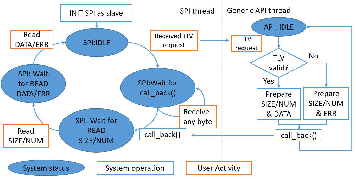
SPI workflow
As shown in the figure above, the DWM1001 SPI thread transfers between four states in serial.
Each state will transfer to its next corresponding state on certain events.
SPI: Idle: the state after initialization and after each successful data transmission/response. Any received data is assumed to be a TLV Request in this state. Thus, on receiving any data, the SPI thread in the firmware passes the received data to the Generic API. The Generic API parses the TLV Requests and prepares the return data.
Waiting for an event: receiving TLV Requests.
Action on an event – if Type == 0xFF:
SPI: Wait for call_back: the DWM1001 SPI waits for the Generic API to parse the TLV Request and prepare the response. Any data from the host side will be ignored and returned with 0x00 in this state.
Waiting for an event: call_back() function is called by the Generic API.
Action on an event:
Toggle Data-Ready GPIO pin HIGH – detailed in SPI Scheme: TLV communication using Data-Ready GPIO pin.
Transfer to “SPI: Wait for READ SIZE/NUM”.
SPI: Wait for Read SIZE/NUM: the DWM1001 SPI has prepared the SIZE byte as a response, and there will be NUM of transfers. SIZE and NUM are a total of 2-byte non-zero data, namely SIZE/NUM. They indicated the total number (i.e. SIZE*NUM bytes) of data or error messages to be responded. The DWM1001 SPI, as a slave, is waiting for the host device to read the SIZE/NUM bytes.
Waiting for an event: the host device reads two bytes.
Action on an event:
Respond with the SIZE/NUM bytes.
Transfer to “SPI: Wait for READ DATA/ERR”.
SPI: Wait for Read DATA/ERR: The DWM1001 SPI has prepared SIZE bytes of data or error messages for each of the NUM transfers as a response to the TLV Request and is waiting for the host device to read it.
Waiting for an event: the host device does NUM transfers. Each transfer should be SIZE bytes. Otherwise, data maybe lost.
Action on an event:
Respond with DATA/ERR.
Toggle Data-Ready GPIO pin LOW – detailed in SPI Scheme: TLV communication using Data-Ready GPIO pin. Transfer to “SPI: Idle”.
In DWM1001, starting from “SPI: Idle”, traversing all four states listed above and returning to “SPI: Idle” indicates a full TLV Request communication flow. The user should have received the response data or error message by the end of the communication flow.
A few different usages and examples are illustrated in the following subsections.
SPI TLV communication using polling
The figure below shows the normal communication flow of a host device writing/reading information to/from the DWM module:
The host device sends the request in TLV format.
The host device reads the SIZE/NUM bytes, indicating the number of transfers to be done and the number of bytes ready to be read in each transfer.
The host device reads SIZE bytes data response in TLV format.
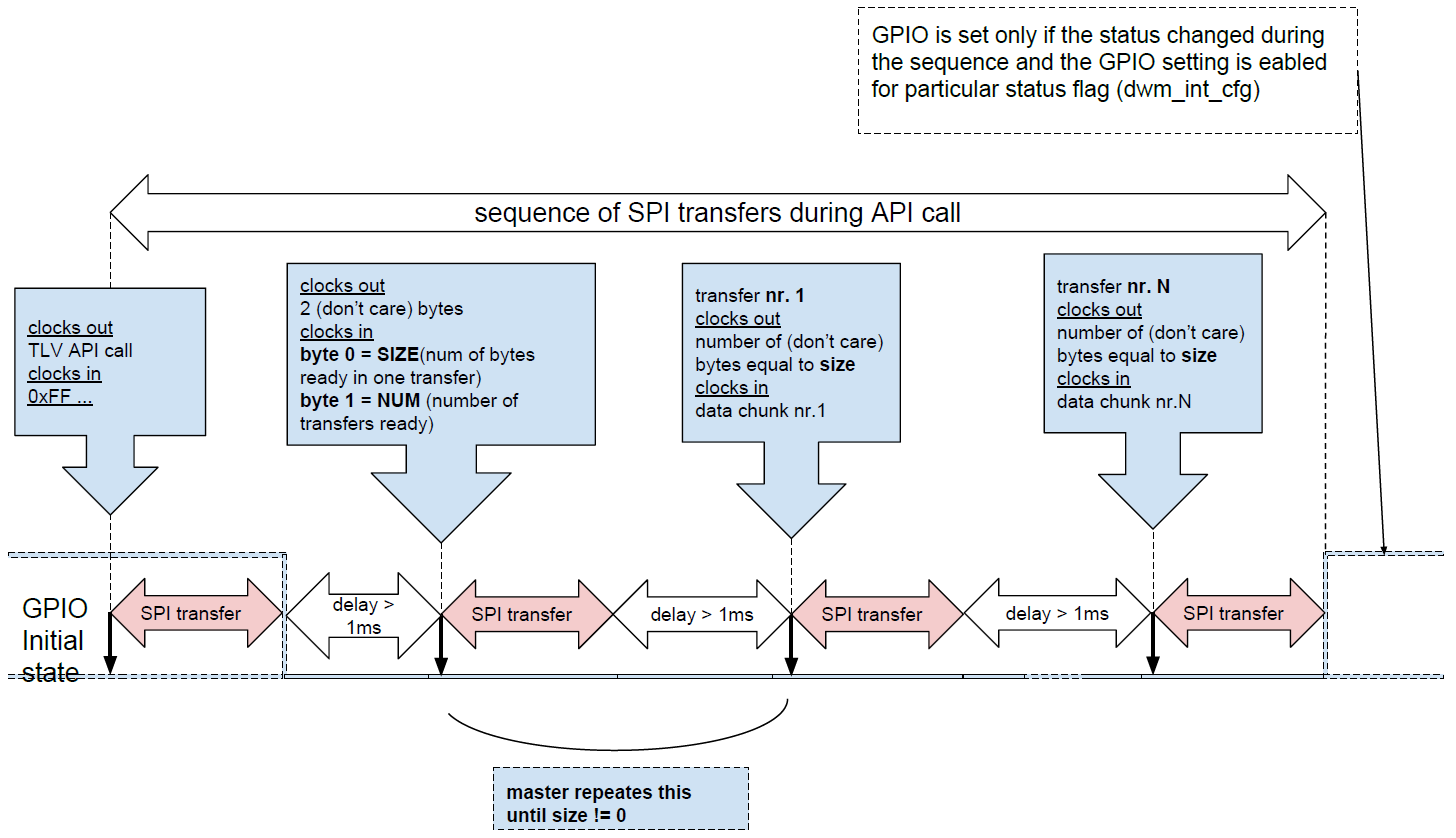
SPI TLV communication using polling
The host device writes the dwm_gpio_cfg_output command to set pin 13 level HIGH in TLV format, 4 bytes in total: Type = 0x28, length = 0x02, value = 0x0D 0x01.
SPI TLV communication using Data-Ready GPIO pin
Users can set up the interrupt Data-Ready GPIO pin (GPIO P0.26) from the DWM1001 to indicate when data is ready, instead of the master polling multiple times to check the response status. When the Data-Ready function is set up, the Data-Ready GPIO pin will be set to LOW level when there’s no data to be read; when the response SIZE/NUM and data are ready to be read, the Data-Ready GPIO pin will be set to HIGH level during states “SPI: Wait for Read SIZE/NUM” and “SPI: Wait for Read DATA/ERR”. Thus, the users can use the Data-Ready GPIO pin as an interrupt or a status pin.
To set up Data-Ready GPIO pin for the SPI scheme, users need to use dwm_int_cfg TLV Request through SPI Scheme: normal TLV communication introduced in SPI TLV communication using polling.
The communication flow of this scheme is illustrated in the figure below.
Set up the SPI interrupt.
The host device writes the request in TLV format.
The host device waits until the Data-Ready GPIO pin on DWM1001 to go HIGH.
The host device reads the SIZE/NUM bytes.
The host device reads the SIZE bytes data response in TLV format in each transfer for NUM times.
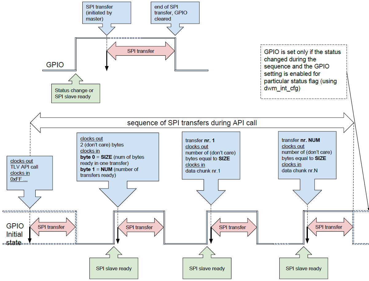
SPI TLV communication using Data-Ready GPIO pin
As can be seen from the steps, this scheme uses the Data-Ready GPIO pin on the DWM1001 to indicate the host device when the response data is ready. This makes the host device less busy in reading SIZE byte.
SPI partial transmission
When reading data from the DWM module, if the host device doesn’t read all bytes of data in one transmission, the reading operation will still be considered done. The rest of the response will be abandoned. For example, in the “SPI: Wait for Read DATA/ERR” state, the DWM module has prepared SIZE bytes of response data and expects the host device to read all SIZE bytes of the response. However, if the host device only reads part of the data, the DWM module will drop the rest and transfer to the next state: “SPI: IDLE”.
SPI error recovery mechanism
The DWM1001 SPI has a special type value 0xFF, called type_nop. A TLV data message with type_nop means no operation. In the “SPI: IDLE” state, when the DWM1001 SPI receives a message and finds the type byte is 0xFF, it will not perform any operation, including sending the TLV data message to the Generic API thread.
The type_nop is designed for error recovery. If the host device is not sure what state the DWM1001 SPI is in, it can make use of the SPI response and the non-partial transmission mechanism and reset the DWM1001 SPI to “SPI: IDLE” state by sending three 0xFF dummy bytes, each in a single transmission. After the three transmissions, the response data from the DWM1001 SPI will become all dummy bytes of value 0xFF, indicating that the DWM1001 SPI is in the “SPI: IDLE” state.
Low-power mode wake-up mechanism
As provided in the PANS library, the DWM module can work in a low-power mode. In the low-power mode, the module puts the API-related threads into a “sleep” state when host devices do not communicate the API . In this case, the host device needs to wake the module through external interfaces before the real communication can start.
For the SPI interface, putting the chip select pin to low level wake ups up the module, i.e. no extra transmission is needed.
After the API transmission has finished, the host device needs to put the module back to “sleep” state to save power, as introduced in dwm_sleep and shell command quit.
SPI wakeup
If DWM sleeps (in low-power mode), the wakeup procedure has to be executed before SPI starts accepting commands. At least a 35 microseconds wide pulse has to be generated on the CS pin of the SPI to wake up from sleep (only in low-power mode).